A brief introduction to FPGAs
Table of Contents
1. Introduction
This document is meant as an introduction to FPGAs. It covers different aspects related to FPGA hardware, architecture and software tools, as well as the various application domains.
FPGAs (Field-Programmable Gate Arrays) are customizable integrated circuits consisting of a network of blocks designed to be configured programmatically post manufacturing. FPGAs can be used to implement solutions to any computable problem (architectural specialization) but they were initially designed to add glue logic between circuit board components. Nowadays, the use cases for FPGAs have broadened due to the advent of Big Data and Machine Learning, and the need for higher data processing performance and customizable hardware.
2. FPGA architecture
Every FPGA comes with a limited number of configurable logic blocks, fixed function blocks (adder, multiplier, …), and I/O blocks that a programmer can arrange into any desired configuration programmatically. The following subsections present the major FPGA components and their key characteristics.
2.1. Logic and fixed function blocks
The most common FPGA block, called configurable logic block - CLB for short, consists of logical cells that can be configured to perform combinatorial functions, to act as a logic gate (i.e. or, and, xor, …) or as a memory block (i.e. D flip-flop or a RAM block). In addition to the CLB, I/O blocks are also implemented to allow the FPGA to communicate with the outside world. All these blocks are connected through a configurable network that allows a very high flexibility and adaptability.
Below (Figure 1) is a diagram showcasing a logic FPGA cell (b) as well as the topology and placement of the main blocks (a).
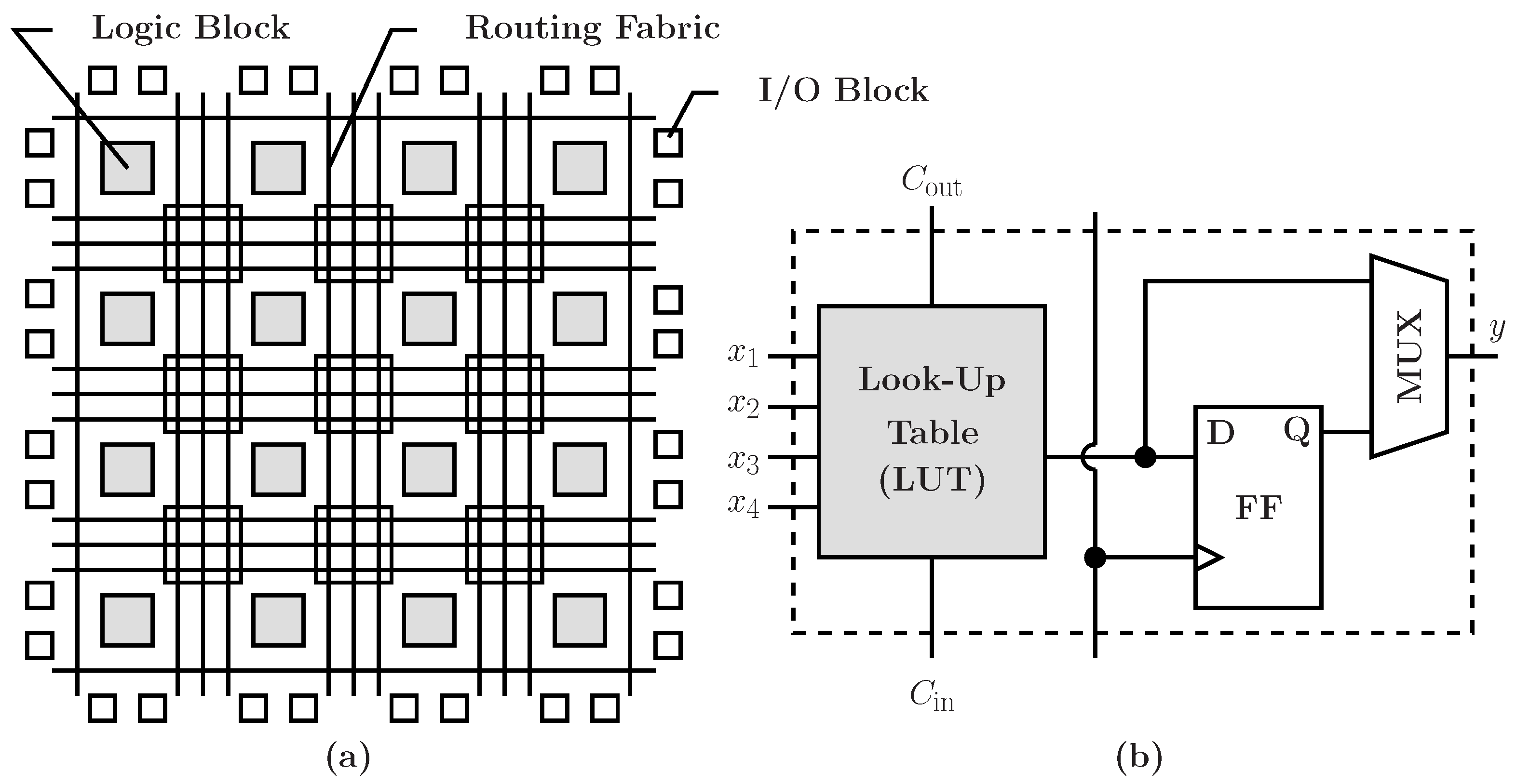
Figure 1: Topology of an FPGA (a), CLB (b)
As we can observe on the figure above, a CLB contains two main elements: a LUT (Look-Up table), and a D flip-flop. Most of the CLB's logic (or, and, xor, …) is implemented as truth tables using SRAM cells in the form of LUTs. The figure below shows the process of implementing a 3-input logic combinatorial function (y = (a & b ) | !c) using a 3-input LUT. For more about how a multiplexer is implemented, see Appendix A.
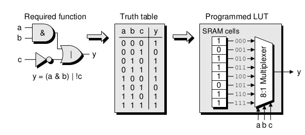
Figure 2: CLB LUT programming
In addition to logic operators, most modern FPGAs offer fixed function blocks in order to enhance performance and allow programmers to use ready-made functional atomic blocks to build larger operations. This is useful for building arithmetic units such as 32-bit adders or multipliers for signal processing. For example, the Xilinx Virtex-5 FPGA comes with prebuilt multiply-accumulate floating-point units aimed at accelerating DSP algorithms (see figure below).
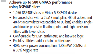
Figure 3: Excerpt from the Virtex-5 FPGA brochure
2.2. Phase-Locked Loop
Another key component of FPGA circuitry is the PLL (Phase-Locked Loop). PLLs are electronic circuits/components that generate an output signal related to the phase of an input signal. Using PLLs, developers can generate multiple frequency domains using an initial frequency source (i.e. a crystal oscillator). The figure below shows a rough diagram of how a PLL can be combined with a frequency divider (here the component divides the frequency by 2) in order to generate a 2000 Hz frequency from an intial 1000 Hz source frequency. For more details about PLLs, see Appendix B.
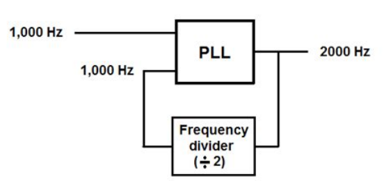
Figure 4: Signal frequency doubling using a PLL
2.3. Logic Elements
Generally, FPGA integrated circuits implement from a few thousands to millions of Logic Elements (or Logic Cells, …). But, this parameter is not usually straightforward for comparing FPGA chips given that each FPGA manufacturer defines what a Logic Element (a Logic Cell, or a slice) represents. For example, Intel defines a MAX10 Logic Element as follows:
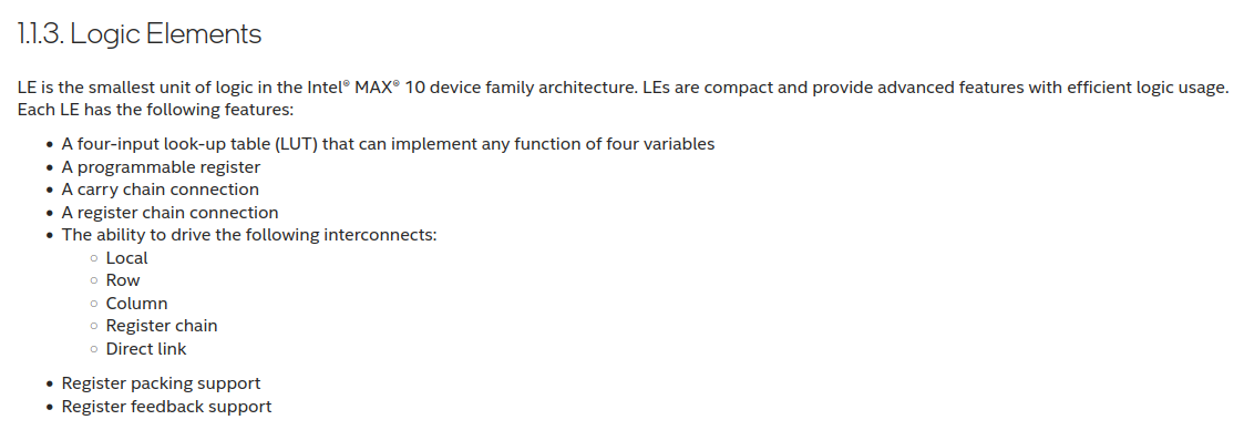
Figure 5: Intel's definition of a Logic Element
This definition may not be accurate (even wrong) when discussing another FPGA chip. In response to this lack of a standard definition, the general consensus in the industry is to use the number of LUTs as a metric for comparing FPGA chips. The more LUTs, the more complex the developer's designs can be. Besides the number of LUTs, other features such as the number and type of arithmetic fixed function blocks, and the number of I/O blocks are crucial in determining if an FPGA chip is the right choice for a certain design or not.
2.4. Parallelism
Parallelism is the ability of a processing unit to operate on multiple blocks of data simultaneously by using a large number of concurrent computing resources. For example, multi-core and many-core CPUs, as well as GPUs, contain multiple independant physical cores running in parallel. Contrary to CPUs, GPUs use a very simple core design allowing for the integration of thousands of cores in a SIMD fashion. SIMD (Single Instruction Multiple Data) is an architectural concept based on processing data by blocks (also called vectors or packets). The figure below (Figure 6) shows the difference between a scalar and a SIMD multiplication:
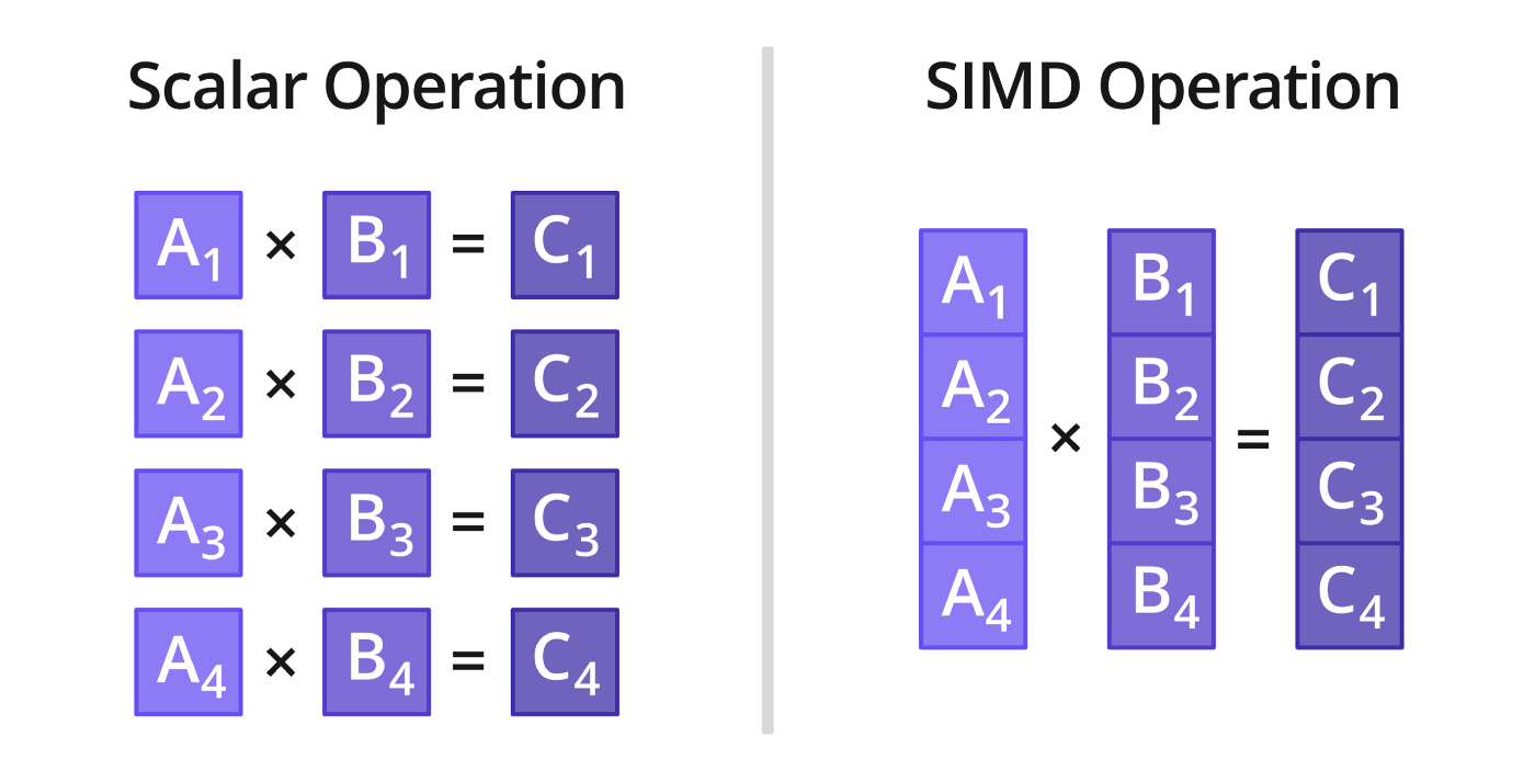
Figure 6: Scalar vs. SIMD
There are different types of parallelism implemented in different chip architectures. Figure. 7 shows the different parallel architectures and how effective they are at exploiting fine-grain paralleslim. In general, each architecture compromises on fine-grain parallelism to accomodate a certain type of compute pattern or workload. Clearly, FPGAs represent the best option for handling parallel or concurrent applications given the large number of logic and I/O blocks available, and the possibility to organize them as needed.
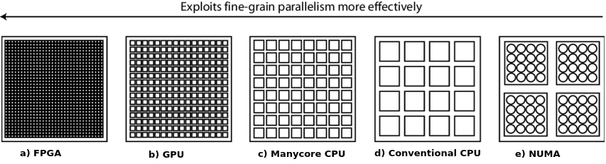
Figure 7: Chip architectures and fire-grain parallelism
The following figure (Figure 8) shows the difference between a scalar DSP unit implementing a dot product operation for 256 input values, and the same operation implemented on a FPGA. We can clearly observe that the parallel nature of the FPGA architecture allows data to flow in independently from multiple I/O blocks (or data lanes) straight into multiple multipliers which then forward the results to an adder that performs the final reduction. The whole process costs around 1 cycle. On the other hand, the DSP performs the operations sequentially requiring 256 cycles to process the whole set of input values. In this case, the FPGA allowed an efficient implementation of the dot product kernel using SIMD parallelism (also called data parallelism) to speed up the execution by a considerable factor: 256x.
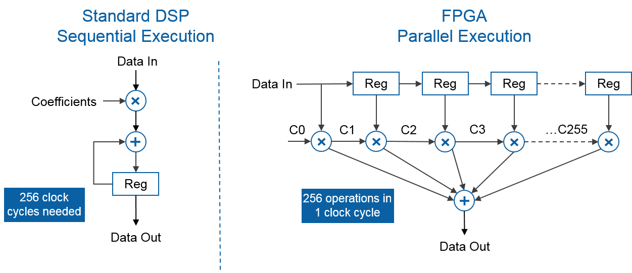
Figure 8: DSP vs. FPGA execution
2.5. Form factors
FPGA chips come packaged in different form factors depending on the application or use case. They can be directly integrated into the circuit board or added as an external device through a high speed connector (Die-to-die interconnect, PCIe, Network, …). In the industrial world, developers generally use development boards and PCIe extension cards to test and validate their prototypical designs. The following sub sections cover the most popular FPGA form factors (devboards and PCIe extensions) and their use cases.
2.5.1. Development boards
- Digilent Arty Z7
Development boards (or devboards) offer a large range of developer-friendly interfaces and tools for rapid prototyping, testing, debugging and tracing. For example, the Digilent Arty Z7 devboard shown below (Figure 9) offers two HDMI ports (input and output), a USB port, a 1 Gpbs Ethernet port, an audio port, and a large set of GPIO ports alongise an SD card reader (at the back of the board). This board also comes with a dual-core ARM Cortex-A9 CPU running at 650 MHz and tightly integrated to the Xiling FPGA that can be easily programmed/debugged using the micro-USB connector. Being afordable and This board was designed for three markets:
- Electronics hobbyists: a niche of tech-savvy consumers re-implementing retro-computer architectures (Z80, 6502, …) in order to run retro games on more efficient modern hardware.
- Video capture and analysis: this board has an input and output HDMI ports
- Academic institutions:
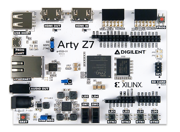
Figure 9: Digilent Arty Z7 FPGA devboard
- Terasic Intel Pathfinder
Another interesting devboard is the Terasic Intel Pathfinder for RISC-V designed for promoting RISC-V software and hardware development. This board comes with a Cyclone IV FPGA containing 114,480 Logic Elements, 3,888 Kbits of embedded memory, and 128 MB of SDRAM. It offers a slew of I/O capabilities for embedded systems development: 2 Ethernet ports, 4 USB ports, TV decoder, RS232 port, …
Figure 10: Terasic Intel Pathfinder for RISC-V board
- Lattice ICEStick
For years, FPGA devices were very expensive and only accessible to those with the financial means to invest in the hardware and the software stack. Nowadays, with the democratisation of electronics, FPGA boards have become more accessible and affordable to the general public. For example, Lattice, an embedded semiconductor and FPGA manufacturer, proposes multiple affordable boards for students, universities, and hobbyists for less than 50$. The board shown below in Figure 11 is the Lattice Icestick HX1K, it costs 48$, is very low-power and comes with 1K LUTs, 5 LEDs, 12 GPIO pins, and an infrared receiver/transmitter.
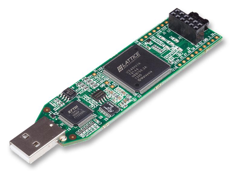
Figure 11: Lattice Icestick HX1K
For more devboards, you can visit the following links:
- Additional ressources
2.5.2. PCIe cards
FPGAs come also in a PCIe card format mainly used for acceleration. These cards can be added to any computer system in order to extend its compute capabilities with custom made designs mainly aiming at accelerating certain compute workloads.
Intel, as well as AMD (Xilinx), offer multiple PCIe FPGA accelerator cards. Below are two examples, the Arria 10GX and the AMD (Xilinx) Alevo U200/U250.
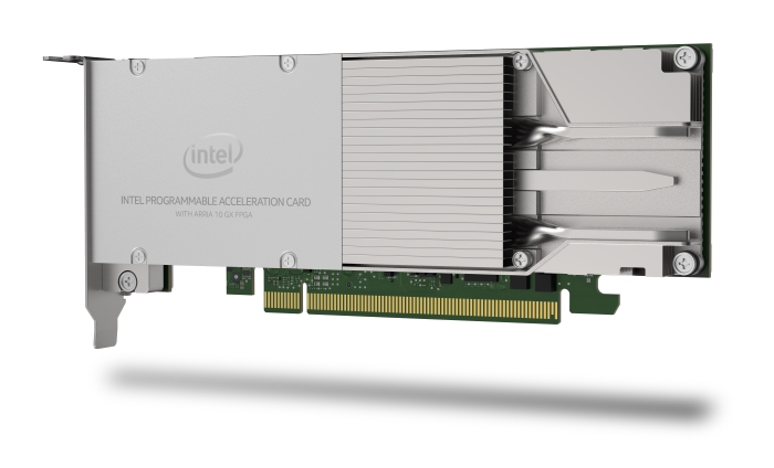
Figure 12: Intel Arria 10GX accelerator card
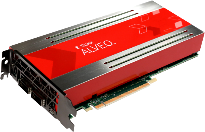
Figure 13: Xilinx Alveo U200/U250
For more information about the Arria 10GX FPGA and the Alveao U200/U250, you can visit Intel's and Xilinx's references:
- https://ark.intel.com/content/www/us/en/ark/products/210381/intel-arria-10-gx-1150-fpga.html
- https://www.xilinx.com/content/dam/xilinx/support/documents/data_sheets/ds962-u200-u250.pdf
The PCIe form factor is mainly used in HPC (High Performance Computing) solutions for accelerating certain specific code patterns with custom hardware. Modern HPC systems using FPGAs for acceleration can be customized programmatically to better fit the computational needs of the target workload. More details on the use of FPGAs in HPC are discussed in the next section.
3. Applications
In the mid to late 1980s, FPGAs were mainly used for allowing circuit board components to communicate while using different communication protocols. For example, an FPGA could be used to interface a device using RS232 with another device using SPI by translating the commands/requests from one protocol to another. This feature was primarily useful for telecommunications and networking devices. Fast forward a decade, FPGAs saw a massive growth in production volume and circuit sophistication, and by the end of 1990s, they had found their way into consumer products as well as automotive and industrial applications.
In this section, we will present some of the key applications that benefited greatly from the advent of FPGAs and their democratization.
3.1. Digital Electronics Design
Digital electronics design is known to be the first discipline to benefit from the high configurability and flexibility of FPGAs. FPGAs allowed electronics engineers to implement, test, and validate their designs before building ASIC (Application Specific Integrated Circuit) chips, enhancing greatly the quality of the designs and pace at which they are updated.
3.2. Digital Signal Processing
Digital signal processing is another field that benefited greatly from FPGAs. Many electronic devices, such as sound cards, were embedding FPGAs within their circuit boards to implement noise filters, and other signal/sound processing algorithms. Generally, and for performance reasons, most signal processing primitives are implemented using DSPs, but in the last few years, given how FPGAs' performace/watt and price range have become more attractive, circuit designers started opting for FPGAs instead of DSPs in order to gain more flexibility and lower their costs.
3.2.1. Sound processing
The advent and evolution of electronics brought numerous devices to the music recording industry. From instruments (like synthetizers) to elaborate studio sound cards and effect pedals, FPGAs have always been part of the circuitry. Most modern studio equipment relies heavily on FPGAs in order to implement certain sound processing algorithms such as equalization, noise filtering, clipping, etc. Usually, such equipment is prototyped using special audio development boards similar to the ones shown below (Coveloz BACH, Audiopraise XMOS). As you can observe, both boards have numerous and diverse audio I/O ports as well as an FPGA. The Coveloz BACH board uses a SoM (System-on-Modue) Cyclone V FPGA from Altera, and the Audiopraise XMOS a Spartan 6 from Xilinx.
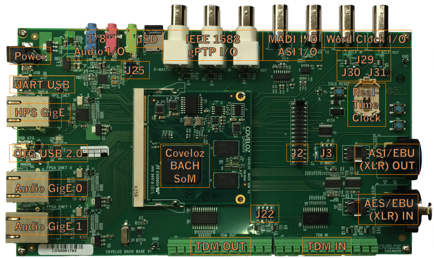
Figure 14: The Coveloz BACH v1 audio analysis board
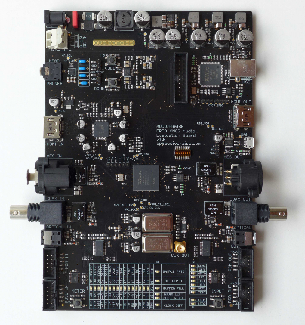
Figure 15: The Audiopraise FPGA XMOS v1 audio board
At the industrial level, multiple vendrors offer different types of hardware. For example, AVID proposes a full sound processing stack for studio recording. Below, is a excerpt from the HDX PCIe card brochure.
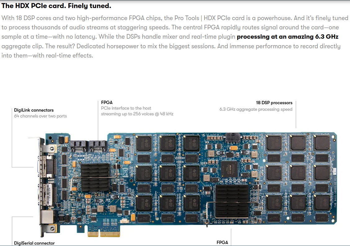
Figure 16: AVID HDX PCIe sound processing card
This card boasts two powerful FPGAs, 18 DSP processors, and 64 input/output channels in a compact PCIe format allowing sound engineers the possibility to apply filters and effects live (in real-time) with very low processing latency, and on multiple input and output channels (https://www.avid.com/products/pro-tools-hdx).
3.2.2. Image/Video processing
Video and image processing is another field where FPGA integration was crucial to the development of modern high quality video recording and processing devices. Many of the devices used by TV production studios, Special Effects studios, Industrial Machine Vision, Medical Imaging, … make extensive use of FPGAs in order to acquire and process video images.
Intel has a very interesting set of articles around the use of FPGAs for Machine Vision and Medical Imaging:
- https://www.intel.com/content/www/us/en/industrial-automation/products/programmable/applications/machine-vision.html
- https://www.intel.com/content/www/us/en/healthcare-it/products/programmable/applications/diagnostic-imaging.html
- https://www.intel.com/content/www/us/en/healthcare-it/products/programmable/overview.html
- https://www.intel.com/content/www/us/en/products/docs/programmable/ai-fpga-whitepaper.html
3.3. Cryptography & Network Security
FPGAs have also been extensively used to implement cryptographic primitives in cases where updatability and security were of major importance. Using FPGAs to implement cryptographic algorithms allows for the algorithms to be updated - a firmware update - when vulnerabilities have been detected. For example, when the hashing algorithms SHA1 and MD5 were broken, many devices using ASICs to implement these primitives were deemed insecure and had to be physically replaced. On the other hand, the devices using FPGAs only needed a firmware update in order to switch to a more secure hashing algorithm. The same happened when the Data Encryption Standard (DES) was broken. Modern systems embed a mix of ASIC cryptochips and FPGAs to implement cryptographic routines.
Another important aspect related to implementing cryptographic primitives using FPGAs is the possibility to implement mitigations and protections against known attacks, such as side-channel attacks, and to update the firmware with new mitigations whenever a new attack is discovered. This is key in order to ensure a high level of implementation security in critical environments (i.e. military applications).
3.4. Artificial Intelligence
3.5. BioInformatics
3.6. HPC
In the last 4 to 5 years, the HPC industry has been growing at a very large pace due to the proliferation of data and compute-intensive applications. Underlying this growth has been a great need for better hardware with lower latency and higher efficiency. This led to the emergence of hardware accelerators to a point where ~80% of today's HPC systems use some form of accelerator (GPU, FPGA, TPU, …). While GPUs have become very popular as accelerators, they are not always the best choice. The primary reason behind the successful integration of GPUs within the HPC stack is parallelism. However, FPGAs are an attractive option capable of delivering equal, if not better performance compared to GPUs due to the fixed architecture of the GPU supporting only SIMD parallelism and requiring batching of the data in order to deliver decent performance. A limitation not shared by FPGAS.
FPGAs are configurable hardware consisting of thousands of logic/compute blocks that a programmer can arrange into any computational construct. With a large number of computing resources available, FPGAs can be configured to support running multiple concurrent programs each processing multiple data blocks concurrently. Therefore, FPGAs can operate on large amounts of data from multiple sources simultaneously (video or audio streams, streams from multiple storage devices or memories, …) offering unique advantages with regards to parallelism over traditional computing architectures.
3.6.1. Memory intensive workloads
In addition to being equipped with DDR4/DDR5 and HBM interfaces allowing for efficient external memory accesses, most modern FPGAs include on-chip memory blocks that can be used to implement high-bandwidth and low frequency data storage. This enables faster data access by reducing the reliance of execution units on external memory. For memory intensive HPC workloads (i.e. simulations), FPGAs can lower the data access overhead in a significant manner.
3.6.2. Communication intensive workloads
FPGAs can be used to implement high-speed/high-bandwidth network interfaces suitable for communication intensive HPC workloads. FPGA-based network interfaces can be particularly beneficial for optimizing distributed and massively parallel applications by allowing the implementation of custom network controllers tailored to an application's needs. Most modern devices come already equipped with 10G Ethernet or SFP interfaces.
3.6.3. Power/Energy efficiency
Being highly programmable, FPGAs allow programmers to choose between different possibilities with regards to power efficiency and performance. Depending on the power/compute budget available, programmers can not only test and fit different designs and implementations to certain constraints, but also implement custom power management where only necessary logic elements are activated. Additionally, FPGAs can exploit parallelism more efficienctly achieving much higher performance per watt than conventional devices. For fixed architectures (CPUs, GPUs, …), the power/performance possibilities are very limited and require some tinkering with hardware parameters, sometimes at the firmware/BIOS level.
4. Programming for FPGAs and software tools
Programming FPGAs is quite a challenging task. First, programmers must have some basic knowledge of signal processing and computer architecture in order to be able to program the devices, troubleshoot, and debug issues. Second, there is a large pool of programming paradigms and languages offering different features and tools. This could be quite overwhelming given that vendors have a tendency to propose feature-full frameworks where one can easily get confused.
This section covers some of the languages and tools available in the market with examples of implementations, in Verilog, of certain basic arithmetic and logic circuits.
4.1. Programming languages
4.1.1. HDL languages
For decades, analog and digital circuits design relied extensively (and still does today) on visual descriptions. Circuits of all sizes were exclusively drawn using CAD tools that generate formated files storing the geometric parameters of a circuit that the designer expressed in a graphical manner. These files were later uploaded to an FPGA's or CPLD's EEPROM memory in order to program it, or as an input to manufacturing equiment (lithography machines, mask generators, …) in order to produce chips, PCBs, …
Nowadays, FPGA devices are programmed almost exclusively using HDLs (Hardware Description Languages). HDLs are procedural textual programming languages that aim at allowing circuit designers to implement their designs using a textual programming logic rather than a visual design approach. Note that visual design tools are still used today for certain basic components and that most CAD tools can generate a visual circuit from HDL and vice-versa. But, for large and complex designs, HDL languages are preferred given that parsing and analyzing text allows for a broader span of features and tools. For a nonexhaustive list of HDL languages you can check here: https://en.wikipedia.org/wiki/Hardware_description_language.
In General, the most widely used HDL programming languages today are Verilog and VHDL. Both languages are heavily influenced by the C programming language syntax and propose a set of primitives and tools that designers can use to produce, verify and test circuits. Verilog and VHDL are standardized by the IEEE. More information on Verilog and VHDL can be found here: Verilog, VHDL.
Below is an example Verilog code implementing a 4-bit counter using 4 LEDs:
module count (input  clk,
              output LED1,
              output LED2,
              output LED3,
              output LED4,
             );

   localparam        BITS = 4; //Counter's bits
   localparam        LOG2DELAY = 16; //Delay

   reg               slowClock = 0; //Slow clock (delayed clock)
   reg [BITS-1:0]    counter = 0;   //4-bit counter
   reg [BITS-1:0]    outcnt = 0;    //4-bit counter
   reg [BITS+LOG2DELAY-1:0] dcounter = 0; //Delay counter

   //
   always @(posedge clk)
     begin
        if (!dcounter)
          slowClock <= !slowClock;

        dcounter <= dcounter + 1;
     end

   always @(posedge slowClock)
     begin
        outcnt <= counter;
        counter <= counter + 1;
     end

   assign { LED1, LED2, LED3, LED4 } = outcnt;

endmodule
4.1.2. OpenCL
For more about OpenCL, check the following links:
- https://en.wikipedia.org/wiki/OpenCL
- https://cpufpga.files.wordpress.com/2016/04/opencl_for_fpgas_isca_2016.pdf (Intel/Altera slides on OpenCL for FPGAs)
- https://arxiv.org/pdf/1810.09773.pdf (PhD: HPC with FPGAs and OpenCL - Hamid Reza Zohouri - Sup. Satoshi Matsuoka)
- https://www.bittware.com/dev/opencl/
- https://educationecosystem.com/blog/fpga-programming-with-opencl/
4.1.3. Python
- fpyga
fpyga is a Python interface allowing for programming Intel/Altera's DE10 devices without having to write RTL-like code (Verilog, VHDL, …). It has no support for other devices.
- pyfpga
pyfpga is also a Python interface but it only handles the tooling management. It can handle the recipes for building (synthesis) and verifying projects written in many languages and using multiple proprietary as well as open source synthesis tools.
- pyRTL
Python-based RTL language. Academic tool!
- pyMTL
Python-based hardware modeling language from Cornell University:
- (deprecated version) https://github.com/cornell-brg/pymtl
- https://github.com/pymtl/pymtl3
- MyHDL
This Python module can generate Verilog and VHDL code from Python based designs.
4.1.4. Verilog example of a Floating-Point unit
The following codes are examples of how certain key elements of a single precision Floating-Point Unit can be implemented in Verilog. These units can be duplicated and bundled up to create a SIMD single precision unit operating on vectors rather than scalars.
- IEEE754 adder
module FloatingAddition #(parameter XLEN=32)
   (
    input [XLEN-1:0]      A,
    input [XLEN-1:0]      B,
    input                 clk,
    output                overflow,
    output                underflow,
    output                exception,
    output reg [XLEN-1:0] result);

   reg [23:0]                                   A_Mantissa, B_Mantissa;
   reg [23:0]                                   Temp_Mantissa;
   reg [22:0]                                   Mantissa;
   reg [7:0]                                    Exponent;
   reg                                          Sign;
   wire                                         MSB;
   reg [7:0]                                    A_Exponent, B_Exponent, Temp_Exponent, diff_Exponent;
   reg                                          A_sign, B_sign, Temp_sign;
   reg [32:0]                                   Temp;
   reg                                          carry;
   reg [2:0]                                    one_hot;
   reg                                          comp;
   reg [7:0]                                    exp_adjust;

   always @ (*)
     begin

        comp =  (A[30:23] >= B[30:23])? 1'b1 : 1'b0;

        A_Mantissa = comp ? {1'b1, A[22:0]} : {1'b1, B[22:0]};
        A_Exponent = comp ? A[30:23] : B[30:23];
        A_sign = comp ? A[31] : B[31];

        B_Mantissa = comp ? {1'b1, B[22:0]} : {1'b1, A[22:0]};
        B_Exponent = comp ? B[30:23] : A[30:23];
        B_sign = comp ? B[31] : A[31];

        diff_Exponent = A_Exponent-B_Exponent;
        B_Mantissa = (B_Mantissa >> diff_Exponent);
        {carry,Temp_Mantissa} = (A_sign ~^ B_sign) ? A_Mantissa + B_Mantissa : A_Mantissa-B_Mantissa;
        exp_adjust = A_Exponent;

        if (carry)
          begin
             Temp_Mantissa = Temp_Mantissa >> 1;
             exp_adjust = exp_adjust + 1'b1;
          end
        else
          begin
             while(!Temp_Mantissa[23])
               begin
                  Temp_Mantissa = Temp_Mantissa << 1;
                  exp_adjust = exp_adjust - 1'b1;
               end
          end

        Sign = A_sign;
        Mantissa = Temp_Mantissa[22:0];
        Exponent = exp_adjust;
        result = { Sign, Exponent, Mantissa };
     end

endmodule
- IEEE754 multiplier
module FloatingMultiplication #(parameter XLEN=32)
   (
    input [XLEN-1:0]      A,
    input [XLEN-1:0]      B,
    input                 clk,
    output                overflow,
    output                underflow,
    output                exception,
    output reg [XLEN-1:0] result);

   reg [23:0]             A_Mantissa, B_Mantissa;
   reg [22:0]             Mantissa;
   reg [47:0]             Temp_Mantissa;
   reg [7:0]              A_Exponent, B_Exponent, Temp_Exponent, diff_Exponent, Exponent;
   reg                    A_sign, B_sign, Sign;
   reg [32:0]             Temp;
   reg [6:0]              exp_adjust;

  always @(*)
     begin
        A_Mantissa = {1'b1, A[22:0]};
        A_Exponent = A[30:23];
        A_sign = A[31];

        B_Mantissa = {1'b1, B[22:0]};
        B_Exponent = B[30:23];
        B_sign = B[31];

        Temp_Exponent = A_Exponent + B_Exponent - 127;
        Temp_Mantissa = A_Mantissa * B_Mantissa;
        Mantissa = Temp_Mantissa[47] ? Temp_Mantissa[46:24] : Temp_Mantissa[45:23];
        Exponent = Temp_Mantissa[47] ? Temp_Exponent + 1'b1 : Temp_Exponent;
        Sign = A_sign ^ B_sign;
        result = {Sign, Exponent, Mantissa};
     end

endmodule
- IEEE754 divider
module FloatingDivision #(parameter XLEN=32)
   (
    input [XLEN-1:0]  A,
    input [XLEN-1:0]  B,
    input             clk,
    output            overflow,
    output            underflow,
    output            exception,
    output [XLEN-1:0] result);

   reg [23:0]         A_Mantissa, B_Mantissa;
   reg [22:0]         Mantissa;
   wire [7:0]         exp;
   reg [23:0]         Temp_Mantissa;
   reg [7:0]          A_Exponent, B_Exponent, Temp_Exponent, diff_Exponent;
   wire [7:0]         Exponent;
   reg [7:0]          A_adjust, B_adjust;
   reg                A_sign, B_sign, Sign;
   reg [32:0]         Temp;
   wire [31:0]        temp1, temp2, temp3, temp4, temp5, temp6, temp7, debug;
   wire [31:0]        reciprocal;
   wire [31:0]        x0, x1, x2, x3;
   reg [6:0]          exp_adjust;
   reg [XLEN-1:0]     B_scaled;
   reg                en1, en2, en3, en4, en5;
   reg                dummy;

   /*----Initial value----*/
   FloatingMultiplication M1(.A({{1'b0,8'd126,B[22:0]}}), .B(32'h3ff0f0f1), .clk(clk), .result(temp1)); //verified
   assign debug = {1'b1, temp1[30:0]};
   FloatingAddition A1(.A(32'h4034b4b5), .B({1'b1,temp1[30:0]}), .result(x0));

   /*----First Iteration----*/
   FloatingMultiplication M2(.A({{1'b0, 8'd126,B[22:0]}}), .B(x0), .clk(clk), .result(temp2));
   FloatingAddition A2(.A(32'h40000000), .B({!temp2[31], temp2[30:0]}), .result(temp3));
   FloatingMultiplication M3(.A(x0), .B(temp3), .clk(clk), .result(x1));

   /*----Second Iteration----*/
   FloatingMultiplication M4(.A({1'b0,8'd126,B[22:0]}), .B(x1), .clk(clk), .result(temp4));
   FloatingAddition A3(.A(32'h40000000),.B({!temp4[31], temp4[30:0]}), .result(temp5));
   FloatingMultiplication M5(.A(x1), .B(temp5), .clk(clk), .result(x2));

   /*----Third Iteration----*/
   FloatingMultiplication M6(.A({1'b0,8'd126,B[22:0]}), .B(x2), .clk(clk), .result(temp6));
   FloatingAddition A4(.A(32'h40000000), .B({!temp6[31],temp6[30:0]}), .result(temp7));
   FloatingMultiplication M7(.A(x2), .B(temp7),.clk(clk),.result(x3));

   /*----Reciprocal : 1/B----*/
   assign Exponent = x3[30:23] + 8'd126 - B[30:23];
   assign reciprocal = {B[31], Exponent, x3[22:0]};

   /*----Multiplication A*1/B----*/
   FloatingMultiplication M8(.A(A), .B(reciprocal), .clk(clk), .result(result));

endmodule
- IEEE754 square root
module FloatingSqrt #(parameter XLEN=32)
   (
    input [XLEN-1:0]  A,
    input             clk,
    output            overflow,
    output            underflow,
    output            exception,
    output [XLEN-1:0] result);

   wire [7:0]         Exponent;
   wire [22:0]        Mantissa;
   wire               Sign;
   wire [XLEN-1:0]    temp1, temp2, temp3, temp4, temp5, temp6, temp7, temp8, temp;
   wire [XLEN-1:0]    x0, x1, x2, x3;
   wire [XLEN-1:0]    sqrt_1by05, sqrt_2, sqrt_1by2;
   wire [7:0]         Exp_2, Exp_Adjust;
   wire               remainder;
   wire               pos;

   assign x0 = 32'h3f5a827a;
   assign sqrt_1by05 = 32'h3fb504f3;  // 1/sqrt(0.5)
   assign sqrt_2 = 32'h3fb504f3;
   assign sqrt_1by2 = 32'h3f3504f3;
   assign Sign = A[31];
   assign Exponent = A[30:23];
   assign Mantissa = A[22:0];

   /*----First Iteration----*/
   FloatingDivision D1(.A({1'b0, 8'd126, Mantissa}), .B(x0), .result(temp1));
   FloatingAddition A1(.A(temp1), .B(x0), .result(temp2));
   assign x1 = {temp2[31], temp2[30:23] - 1, temp2[22:0]};

   /*----Second Iteration----*/
   FloatingDivision D2(.A({1'b0, 8'd126, Mantissa}), .B(x1), .result(temp3));
   FloatingAddition A2(.A(temp3), .B(x1), .result(temp4));
   assign x2 = {temp4[31], temp4[30:23] - 1, temp4[22:0]};

   /*----Third Iteration----*/
   FloatingDivision D3(.A({1'b0,8'd126, Mantissa}), .B(x2), .result(temp5));
   FloatingAddition A3(.A(temp5), .B(x2), .result(temp6));
   assign x3 = {temp6[31], temp6[30:23] - 1, temp6[22:0]};
   FloatingMultiplication M1(.A(x3), .B(sqrt_1by05), .result(temp7));

   assign pos = (Exponent>=8'd127) ? 1'b1 : 1'b0;
   assign Exp_2 = pos ? (Exponent-8'd127) / 2 : (Exponent - 8'd127 - 1) / 2 ;
   assign remainder = (Exponent - 8'd127) % 2;
   assign temp = {temp7[31], Exp_2 + temp7[30:23], temp7[22:0]};
   FloatingMultiplication M2(.A(temp), .B(sqrt_2), .result(temp8));
   assign result = remainder ? temp8 : temp;

endmodule
4.1.5. RISC-V cores
There is a plethora of RISC-V cores implementations on the web. Some are centered around teaching and academic use, others are more centered around deployment on embedded environments. So far, most of the open source implementations target the RV32I (base integers instruction set) which only implements certain basic operations (add, sub, mul, or, and, …) in 32-bit mode. On https://opencores.org, there are many projects implementing various chips (DSPs, CPUs, AI accelerators, …) using the RISC-V instruction set, unfortunately, most of these designs are not production grade and are mostly toy projects.
4.2. Software tools
4.2.1. Vendor tools
4.2.2. Open Source FPGA centered projects
5. References
- https://www.tomshardware.com/news/amd-to-fuse-fpga-ai-engines-onto-epyc-processors-arrives-in-2023
- https://www.intel.com/content/www/us/en/developer/articles/technical/comparing-cpus-gpus-and-fpgas-for-oneapi.html#gs.q5yjcp
- https://www.intel.com/content/www/us/en/docs/programmable/683521/21-4/fpga-overview.html
6. Appendix A
The following diagram shows an implementation of a digital 8 to 1 (8:1) multiplexer using logic gates. This multiplexer takes 3 selection inputs (s(0), s(1), s(2)) and outputs the selected value from a set of 8 inputs (I(0) to I(7)).
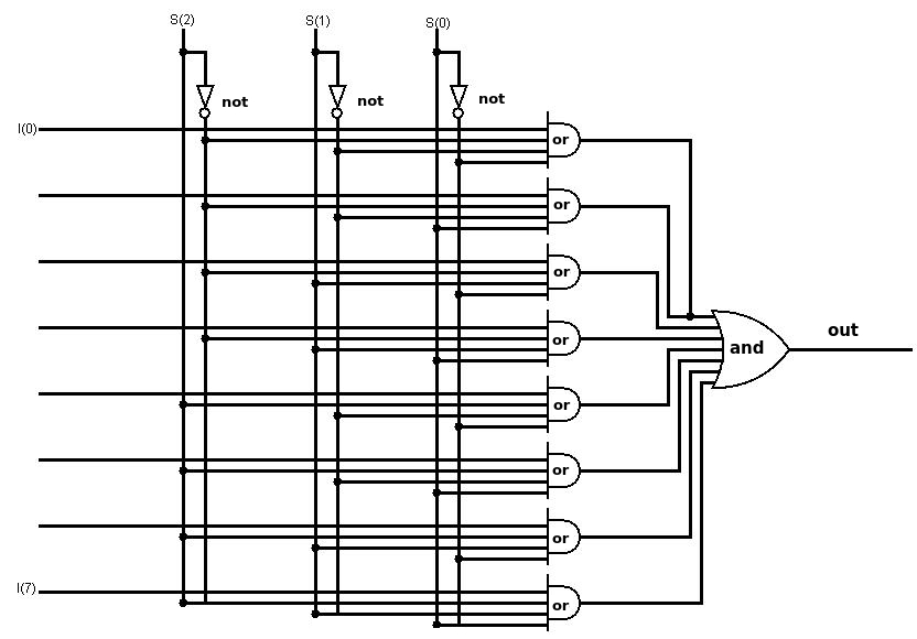
Figure 17: Digital 8:1 multiplexer
7. Appendix B
The following is a circuit diagram showcasing how a PLL is implemented.
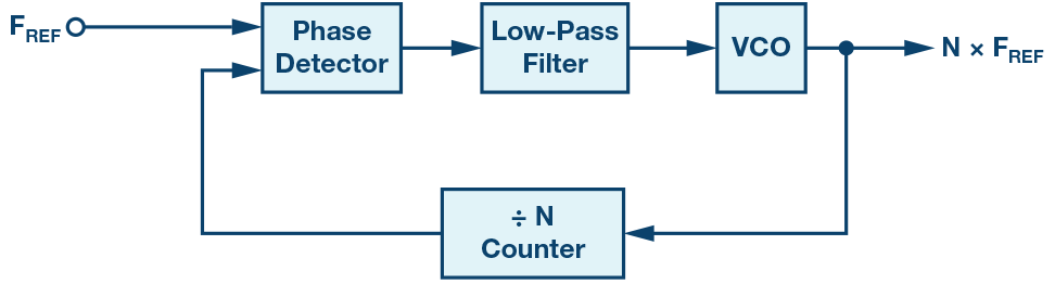
Figure 18: PLL circuit implementation